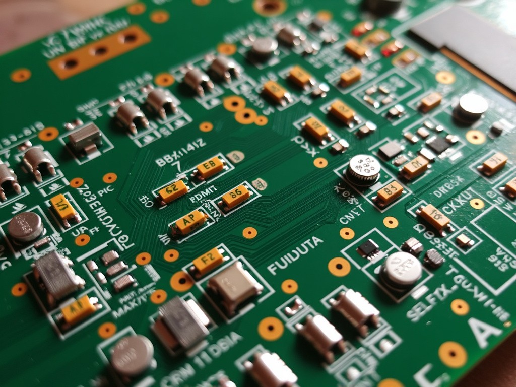
Power electronics are crucial in modern systems, where PCB design directly impacts performance and reliability. Effective design is necessary for managing heat, ensuring signal integrity, and reducing parasitic effects, all of which are critical in power applications. At the core of these systems, OurPCB Design ensures high-quality, manufacturable PCB layouts that reduce errors and optimise efficiency. This focus on thermal management, routing, and power integrity is essential to achieving optimal performance in high-power environments.
Why PCB Design Matters in Power Electronics
Power electronics deal with the control and conversion of electrical power, and in many cases, these systems handle large amounts of energy. A poorly designed PCB can lead to issues such as overheating, signal interference, and even complete system failure. To mitigate these risks, working with professional electronic design services can ensure that power handling, thermal management, and signal integrity are optimized, resulting in a more efficient and reliable design. Therefore, the design of the PCB is crucial to the performance, safety, and longevity of power electronics systems.
Here are a few reasons why PCB design is essential in power electronics:
Heat Dissipation and Thermal Management
Power electronic devices, such as power converters, inverters, and rectifiers, often handle high currents, which generate significant amounts of heat. Effective PCB design ensures that heat is managed properly. Components such as power transistors and inductors require specific placement on the PCB to optimise heat dissipation.
The design must include elements like thermal vias, heat sinks, and proper material choices to ensure that the heat generated by the components is evenly distributed and dissipated. Poor thermal management can lead to component damage and reduced efficiency, particularly in high-power applications.
Power Integrity and Signal Integrity
Maintaining power and signal integrity is one of the most critical aspects of PCB design in power electronics. Power integrity ensures that the power supplied to the components remains stable, even as loads change dynamically. On the other hand, signal integrity ensures that data transmitted through the PCB is not distorted by noise, voltage fluctuations, or electromagnetic interference (EMI).
Effective PCB layout techniques, such as controlling trace widths and separating power and signal layers, help maintain both power and signal integrity. Shielding techniques like ground planes and guard rings are also employed to minimise noise and prevent interference, ensuring the system performs as expected under various conditions.
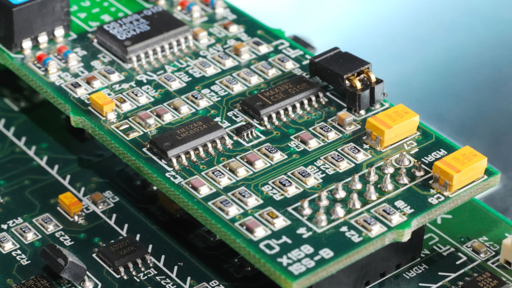
Component Placement and Routing
The arrangement of components and the routing of traces are pivotal for minimising resistance, inductance, and capacitance, all of which affect performance in power electronic systems. A well-designed PCB ensures that the components are placed in a way that minimises current loops and reduces electromagnetic interference. This placement can also reduce power losses, which is crucial for energy-efficient designs.
In high-power systems, short and direct routing paths for high-current traces are essential to minimise parasitic inductance and resistance. Designers must carefully manage the routing of signals and power to avoid crosstalk and signal degradation.
Minimizing Parasitic Effects
Parasitics—unintended inductance, capacitance, and resistance—are significant challenges in power electronics. Parasitic inductance in power traces can result in unwanted oscillations and voltage spikes, while parasitic capacitance can cause signal degradation. These effects become even more pronounced in high-frequency power electronics systems.
To mitigate parasitic effects, PCB designers must carefully consider the layout, focusing on reducing the length of high-current traces, optimizing trace widths, and ensuring adequate spacing between critical components. This reduces unwanted inductive and capacitive coupling that can affect the performance of the entire system.
Efficient Use of Space
Power electronics often have to be compact, especially in applications such as electric vehicles or portable consumer devices. Space constraints make it essential for PCB designers to optimize the use of the available area. Components must be strategically placed to minimize the size of the board while ensuring there is adequate space for heat dissipation and signal routing.
Using multi-layer PCBs is one way to efficiently manage space.
By adding more layers, designers can separate power and signal traces, manage thermal properties better, and allow for more complex routing, leading to improved overall performance in a compact form factor.
High Current and Voltage Handling
PCBs in power electronics need to handle high currents and voltages, sometimes exceeding 100 amps or even several kilovolts. Designing PCBs for these power levels requires careful material selection and trace design. Thicker copper layers, wide traces, and plated through-holes (PTHs) can help manage high currents, while careful component selection ensures that high voltage levels are properly insulated.
Additionally, the designer must account for voltage clearance, which refers to the space required between conductive components to avoid arcing or short circuits. High-voltage designs require larger clearances between traces and components to ensure safe operation.
Electromagnetic Compatibility (EMC) and Electromagnetic Interference (EMI)
Electromagnetic interference (EMI) is a critical challenge in power electronics, where switching components can generate high-frequency noise that affects nearby systems. To maintain electromagnetic compatibility (EMC), PCB design must incorporate features that reduce EMI emissions and protect the system from external interference.
Techniques such as grounding, shielding, and proper layer stack-up are essential. Careful routing of high-speed signals and the use of filtering components like ferrite beads or capacitors can also help in reducing EMI.
Reliability and Durability
In power electronics, reliability is non-negotiable, especially in mission-critical applications such as aerospace, automotive, or industrial systems. PCB design has a direct impact on the reliability and durability of power electronic systems. Designers must ensure that components and traces can withstand the environmental stresses they will face, such as temperature fluctuations, mechanical shocks, and vibrations.
The use of robust materials, high-reliability components, and design practices like derating (operating components below their maximum ratings) can significantly enhance the long-term reliability of the system.
Key Considerations for PCB Design in Power Electronics
To summarize the importance of PCB design in power electronics, here are a few key considerations designers must keep in mind:
- Thermal Management: Implement heat sinks, thermal vias, and use high-quality materials to manage heat effectively.
- Signal and Power Integrity: Use appropriate shielding, ground planes, and keep power and signal layers separate to ensure stable operation.
- Component Placement and Routing: Place components to minimize parasitics and ensure efficient routing.
- Space Management: Use multi-layer PCBs to manage complex designs within limited space.
- High Power Handling: Use thick copper layers, wide traces, and adequate clearances to manage high currents and voltages.
- EMI/EMC: Incorporate design strategies to mitigate EMI and ensure the board complies with EMC standards.
- Reliability: Design with long-term reliability in mind, considering both environmental conditions and system demands.
Conclusion
In power electronics, the role of PCB design is critical in ensuring the overall performance, safety, and efficiency of the system. A well-designed PCB not only manages power and heat efficiently but also helps to reduce noise, improve signal integrity, and ensure the system can handle high currents and voltages. As power electronic applications continue to evolve, the importance of effective PCB design will only increase, and companies like OurPCB play a pivotal role in providing reliable and high-quality PCB solutions for these advanced systems.